
Introduction
Consumer electronic products have penetrated into our daily life, from smart phones, tablet PCs to smart home appliances and wearable devices, the speed of its renewal is amazing. What supports the powerful functions of these products is the highly integrated PCBA inside, so it is especially important to control the quality of PCBA.
In the face of huge market demand and fierce competition, PCBA testing for consumer electronics products faces unique challenges: ensuring high product quality and a favorable user experience, while balancing extremely high yields, strict cost control, and fast time-to-market cycles. Therefore, it is critical to develop and implement efficient and comprehensive PCBA test solutions.
I. The test of consumer electronics PCBA has distinct industry characteristics
1. High yield and cost-sensitive: consumer electronics products are usually produced in millions or even millions of scale, which means that the test process must be extremely fast and automated, the test cost needs to be controlled to the minimum to ensure the competitiveness of the overall product.
2. Functional diversity and high integration: In order to achieve rich functionality in a limited space, consumer electronics PCBAs are often designed with a high degree of integration, including complex processors, storage, wireless communication modules, sensor interfaces, etc., which makes test coverage and troubleshooting more complex.
3. Short product life cycle: market demand changes rapidly, new products come out in an endless stream, requiring test solutions can be quickly developed, deployed and adapted to different models of products, to shorten the cycle of building the test system.
4. User experience concerns: the product's response speed, connection stability, battery life, human-computer interaction, such as smoothness, etc. have a direct impact on the user experience, these performance indicators need to be verified at the PCBA level.
5. Reliability requirements: consumers expect the product can be used stably for several years, withstand the test of the daily environment, which requires the test program can screen out potential early failure risk.

II. in order to meet these challenges, the consumer electronics field has formed a multi-level, comprehensive PCBA test solution system, designed to maximize the defect capture rate in the most cost-effective way.
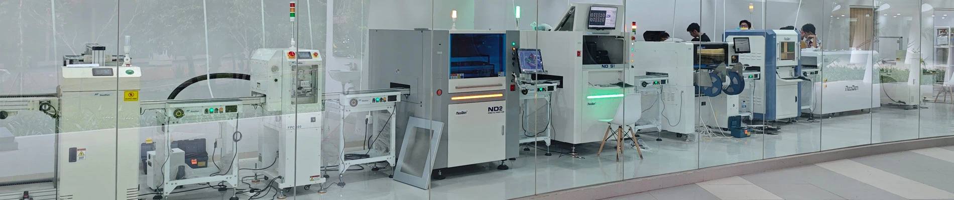
1. SMD production line production process testing: this is the first line of defense to ensure the quality of PCBA processing, immediately after the completion of PCBA assembly.
- Solder Paste Inspection machine (SPI): Checks the volume, area and thickness of solder paste printing to detect soldering hazards in advance.
- Automatic Optical Inspection machine (AOI): High-speed visual inspection of whether the components are correctly mounted, whether the polarity is correct, whether there are leakage, wrong parts and basic welding defects. It is a very effective means of first round screening in mass production.
- X-ray inspection machine (X-ray): used to check the quality of BGA, QFN and other packages can not directly see the quality of the solder joints, especially important in high-density PCBA.
2. In-circuit test (ICT): Through the "bed of pins" fixture contact test points on the PCBA, rapid detection of open and short circuits, components (such as resistance, capacitance, inductance) value and polarity, as well as simple digital circuit functions. ICT is very effective for quickly locating assembly defects and component failures introduced by PCBA processing, and is widely used in mass production.
3. Flying Probe Testing: The use of multiple movable probes for testing, without the need for expensive needle bed fixtures. It is more suitable for prototype development, small batch production or PCBA with insufficient test points for ICT, although the speed is relatively slower than ICT, but its flexibility is high.
4. Functional Test: This is a key part of verifying the functionality and performance of PCBAs under simulated real-world operating conditions.
FCT solutions are usually highly automated and customized to simulate the PCBA's operating environment in the final product, such as connecting simulated displays, buttons, sensors, power loads, and so on.
Tests include: processor boot, memory read/write, communication interface (USB, SPI, I2C, UART) functionality, power management unit control, basic wireless module (Wi-Fi, Bluetooth) functionality, and more.
Part of the program will also include the PCBA firmware burning and basic verification.
5. System-level functional testing: Although strictly speaking is part of the whole machine test, but the PCBA ultimately to be integrated into the whole machine work. System-level testing in the machine environment can identify compatibility issues between PCBAs or between PCBAs and structural components, and is an important part of ensuring the end-user experience.
III. in consumer electronics, a successful PCBA test program is the art of balancing efficiency and quality. The keys to achieving this balance are.
- Early Defect Capture: Maximize the use of manufacturing process inspection (SPI, AOI, X-ray, ICT) to detect and reject defects at an early stage after PCBA processing is complete, significantly reducing subsequent testing and rework costs.
- Automation and Parallel Testing: The extensive use of automated test equipment (ATE) and the realization of parallel testing through cleverly designed test fixtures dramatically improves test efficiency and meets high throughput requirements.
- Design for Testability (DFT): Fully consider test requirements at the early stage of product and PCBA design, and work closely with the PCBA processing team to ensure that the design has good testability, such as reserving enough test points, introducing boundary scan, etc., so as to simplify the test program and reduce the test cost.
- Data Analysis and Process Improvement: Continuously collect and analyze test data (e.g., pass rate, failure types), locate the root causes of defects, and provide feedback to the design and PCBA processing links to promote continuous process improvement and improve the overall efficiency and quality of manufacturing and testing.
Summarize
The PCBA test solution for consumer electronics is the integration of multiple technologies and optimization of strategies. It needs to ensure high quality and user experience while meeting the market demand of large-scale, low-cost, and rapid iteration. This requires test solutions that are efficient, automated, and have adequate coverage. And all this is based on high-quality PCBA processing. Only by closely combining advanced manufacturing processes with scientific test solutions can we stand invincible in the fierce consumer electronics market and bring superior product experiences to consumers around the world.

Company profile
Zhejiang NeoDen Technology Co., LTD., founded in 2010, is a professional manufacturer specialized in SMT pick and place machine, reflow oven, stencil printing machine, SMT production line and other SMT Products. We have our own R & D team and own factory, taking advantage of our own rich experienced R&D, well trained production, won great reputation from the world wide customers.
In this decade, we independently developed NeoDen4, NeoDen IN6, NeoDen K1830, NeoDen FP2636 and other SMT products, which sold well all over the world. So far, we have sold more than 10,000pcs machines and exported them to over 130 countries around the world, establishing a good reputation in the market. In our global Ecosystem, we collaborate with our best partner to deliver a more closing sales service, high professional and efficient technical support.