
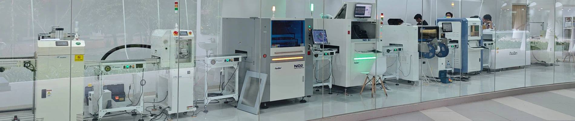
With the enhancement of environmental protection awareness, countries have become more and more stringent on the control of hazardous substances in electronic products. In the PCBA processing industry, the application of lead-free process has become an important initiative to promote environmental protection. In this article, we will discuss the contribution of PCBA factories adopting lead-free process to environmental protection, how to reduce the negative impact on the environment and promote sustainable development.
1. What is lead-free process?
Lead-free process refers to the use of lead-free materials (e.g., lead-free solder) to replace the traditional lead-containing solder in the PCBA processing process. Since lead is a heavy metal that is harmful to human body and the environment, the use of lead-free materials can effectively reduce the hazards of electronic products to the environment and human health. Lead-free process is an important measure to respond to the global environmental protection policy, but also to ensure that products comply with RoHS (Restriction of Hazardous Substances Directive) and other environmental standards.
2. Reducing Lead Pollution to the Environment
Lead is a commonly used material in the traditional soldering process, especially in PCBA processing, lead solder is widely used for circuit board connections. Once lead leaks into the environment, especially at the end-of-life stage of electronic products, it will pollute soil, water and air and jeopardize the ecosystem. The implementation of the lead-free process effectively reduces the pollution of lead to the environment, avoids the accumulation of lead in electronic waste, and reduces the pressure on environmental governance.
The use of lead-free solder can significantly reduce the toxic substances in e-waste and meet the requirements of increasingly stringent global environmental regulations. Lead-free solder usually uses tin, copper, silver and other materials, not only reduces the use of lead, but also improves the environmental performance of the product.
3. Improve product recyclability
The lead-free process enhances the recycling rate of PCBA products. In the traditional leaded soldering, due to the presence of lead, e-waste recycling is more difficult, and the recycling process may produce harmful gases. The solder material used in the lead-free process is more environmentally friendly, meets the recycling requirements, and the environmental burden in the recycling process is smaller. Therefore, PCBA products using lead-free solder are easier to recycle and reduce the long-term impact of waste on the environment.
In addition, with the popularity of lead-free materials, the related recycling technology is also being optimized, providing more environmentally friendly solutions for e-waste disposal.
4. Compliance with international environmental regulations
As global environmental regulations become stricter, countries are making clear requirements for hazardous substances in electronic products. RoHS (Restriction of Hazardous Substances Directive) requires that the use of certain hazardous substances in products be banned or restricted, and lead is one of them. In order to meet RoHS standards, PCBA factories must use lead-free processes instead of lead-containing processes. This not only helps product compliance, but also enhances the factory's environmental image.
By implementing lead-free processes, PCBA factories can better adapt to the environmental requirements of the global market, meet customer demand for environmentally friendly products, and enhance market competitiveness. At the same time, this also lays the foundation for future compliance and sustainable development in the field of environmental protection.
5. Technical Challenges and Development Prospects of Lead-Free Processes
Despite the significant advantages of lead-free processes in terms of environmental protection, they also face certain technical challenges in practical application. For example, the higher melting point of lead-free solders requires factories to use higher-temperature soldering equipment, which may increase production costs and place greater demands on the durability of the equipment. In addition, lead-free solders have different properties from traditional leaded solders, which may affect solder quality and require factories to be more sophisticated in process design and control.
With the development of technology, more and more lead-free materials and soldering techniques have been applied to solve these technical difficulties. In the future, with the continuous improvement of the process, the lead-free process will be more mature, and the cost is expected to be further reduced to provide PCBA factories with more economical and environmentally friendly production solutions.
Conclusion
The application of lead-free process in PCBA processing is a key step in promoting environmental protection. It not only effectively reduces the environmental pollution caused by lead and improves the recyclability of products, but also helps PCBA factories to meet the requirements of international environmental regulations. Despite the challenges in technical implementation, the popularization of lead-free process will further promote the green development of the electronics industry and sustainable manufacturing as the process continues to advance. For PCBA factories, the adoption of lead-free process is not only the need to comply with regulations, but also a necessary way to realize environmentally friendly production and enhance enterprise competitiveness.

Quick facts about NeoDen
1. Established in 2010, 200+ employees, 8000+ Sq.m. factory.
2. NeoDen products: Smart series PNP machine, NeoDen N10P, NeoDen9, NeoDen K1830, NeoDen4, NeoDen3V, NeoDen7, NeoDen6, TM220A, TM240A, TM245P, reflow oven IN6, IN12, IN12C, Solder paste printer FP2636, PM3040.
3. Successful 10000+ customers across the globe.
4. 30+ Global Agents covered in Asia, Europe, America, Oceania and Africa.
5. R&D Center: 3 R&D departments with 25+ professional R&D engineers.
6. Listed with CE and got 50+ patents.
7. 30+ quality control and technical support engineers, 15+ senior international sales, timely customer responding within 8 hours, professional solutions providing within 24 hours.