

Introduction
The wave of the Internet of Things (IoT) is sweeping across the globe at an unprecedented pace. From smart homes and wearable devices to industrial automation and smart cities, the interconnection of all things is becoming a reality. Within this complex network, the "heart" of every smart device is its internal PCBA (Printed Circuit Board Assembly). Consequently, the rapid development of IoT imposes higher demands on traditional PCBA manufacturing techniques, driving profound technological innovation.
I. New Challenges for PCBA Manufacturing in IoT
IoT devices typically exhibit several key characteristics that directly challenge conventional PCBA manufacturing models:
1. High Density and Miniaturization
To meet the slim and lightweight requirements of wearable devices and sensor nodes, IoT PCBA designs are becoming increasingly compact. This necessitates increasingly smaller component packages, such as the widespread adoption of micro-components like 01005 and 0201. Simultaneously, PCB boards feature increased layer counts, narrower trace widths and spacing, and finer via diameters. These factors pose significant challenges to the placement accuracy of pick and place machines, the soldering reliability of reflow oven / wave soldering oven processes, and PCB manufacturing techniques.
2. Low Power Consumption and High Reliability
Many IoT devices rely on battery power and require long-term stable operation. This necessitates not only extremely low power consumption in PCBA design but also heightened reliability in harsh environments. For instance, outdoor sensor nodes must withstand extreme temperatures, humidity, and vibration. Consequently, PCBA manufacturing must employ high-reliability materials and processes, such as substrates resistant to high and low temperatures, high-reliability solder, and conformal coating techniques.
3. Multifunctional Integration and Mixed Packaging
To achieve richer functionality, IoT PCBA often requires integrating multiple component types, such as RF modules, MEMS sensors, microcontrollers, and power management chips. This increases design and manufacturing complexity, necessitating mixed placement of diverse packaging forms (e.g., BGA, QFN, CSP) and even advanced packaging technologies like SiP (System-in-Package).
II. The Path of Innovation in PCBA Processing Technology
To address these challenges, the PCBA processing industry is advancing technological innovation in the following directions:
1. Upgrading and Intelligentization of SMT Equipment
Traditional SMT placement machines struggle to meet the placement demands of micro-components. New-generation SMT equipment offers higher placement accuracy, faster placement speeds, and more robust vision recognition systems. Simultaneously, reflow ovens require more precise temperature control to accommodate lead-free solder and the soldering demands of micro-components. These devices typically integrate sensors and data analytics capabilities, enabling more accurate process control and predictive maintenance.
2. Application of High-Precision Soldering and Inspection Technologies
To ensure the reliability of minute solder joints, the industry is widely adopting novel soldering techniques and more sophisticated inspection methods. For instance, higher-precision printers control solder paste volume, while vacuum reflow processes minimize solder voids. Beyond traditional AOI inspection, 3D-SPI (3D solder paste inspection) and AXI (automated X-ray inspection) are increasingly deployed to verify solder joint quality beneath BGAs, LGAs, and other packages.
3. The Rise of Digitalization and Flexible Manufacturing
In the IoT era, product lifecycles are shorter, and orders increasingly favor "small batches, multiple varieties." This demands greater flexible manufacturing capabilities from PCBA production lines. By integrating MES (Manufacturing Execution Systems) and industrial IoT technologies, factories can achieve real-time monitoring and traceability of production data, rapidly switch between product models, and optimize production scheduling based on data analysis-enhancing efficiency and responsiveness.
Conclusion
The development of IoT presents unprecedented opportunities and challenges for the PCBA processing industry. This technological revolution represents not only an upgrade of production equipment but also a fundamental reshaping of manufacturing philosophy. Only enterprises that actively embrace high-density, high-precision, high-reliability, and flexible manufacturing will seize opportunities amid the IoT wave, becoming core forces empowering the future of universal connectivity.
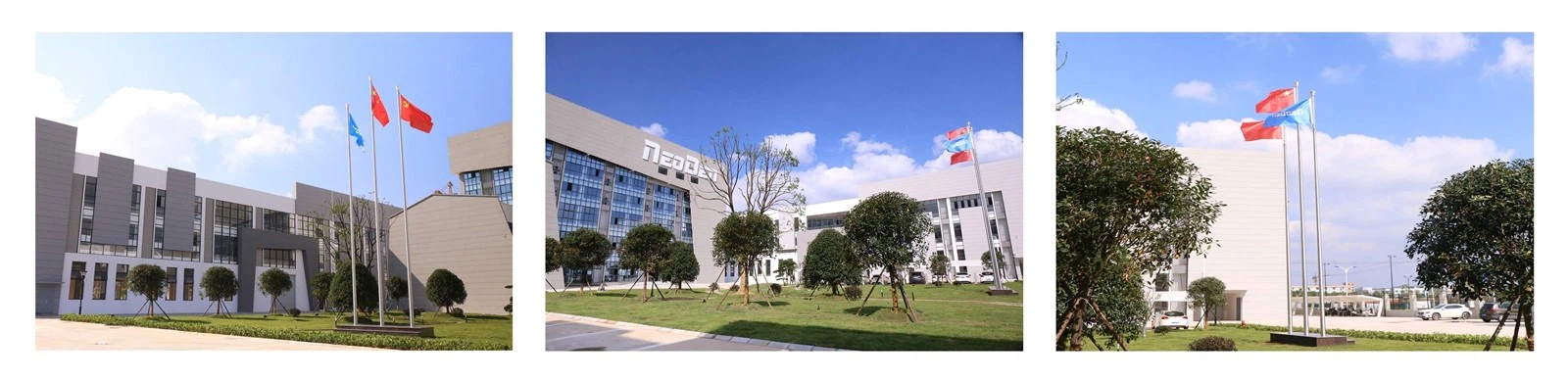
Quick facts about NeoDen
1) Established in 2010, 200 + employees, 27000+ Sq.m. factory.
2) NeoDen Products:Different Series PnP machines, NeoDen YY1, NeoDen4, NeoDen5, NeoDen K1830, NeoDen9, NeoDen N10P. Reflow Oven IN Series, as well as complete SMT Line includes all necessary SMT equipment.
3) Successful 10000+ customers across the globe.
4) 40+ Global Agents covered in Asia, Europe, America, Oceania and Africa.
5) R&D Center: 3 R&D departments with 25+ professional R&D engineers.
6) Listed with CE and got 70+ patents.
7) 30+ quality control and technical support engineers, 15+ senior international sales, for timely customer responding within 8 hours, and professional solutions providing within 24 hours.