

Introduction
In the field of modern electronics manufacturing (EMS/SMT), PCBs are rapidly evolving toward higher density and miniaturization (such as 01005 and 008004 components, as well as fine-pitch BGAs). As pad spacing continues to shrink, the precision required for solder paste printing has reached the micrometer level.
Industry statistics show that of all soldering defects on SMT production lines, more than 60% to 70% originate from the solder paste printing stage.
To intercept defects early in production, reduce rework costs, and improve process yield, solder paste inspection equipment has become an indispensable core quality control component in automated SMT production lines.
What Does SMT SPI Equipment Do?
1. SPI Is Primarily Used for Solder Paste Printing Quality Inspection
SPI equipment is specifically designed to inspect the quality of solder paste on PCBs after printing. Its core function is to perform morphological analysis and data quantification of the solder paste on PCB pads using a high-precision vision inspection system-after solder paste printing is complete and before component placement.
It is important to note that SPI inspects the "solder paste printing results," not the electronic components themselves.
2. Why is inspection necessary after solder paste printing?
In traditional SMT production, visual inspection or relying solely on printer parameters cannot accurately quantify the three-dimensional volume and height of the solder paste. If a printing defect exists and is not detected in time, the circuit board will proceed to the component placement and reflow soldering processes. Issues such as short circuits, tombstones, insufficient solder, or voids that form after soldering can cause rework costs to skyrocket and may even result in the board being scrapped.
SPI can immediately detect the following common printing anomalies:
- Solder paste position offset
- Abnormal solder paste volume (Volume Too High/Low)
- Abnormal solder paste area (Area Too Large/Small)
- Abnormal solder paste height (Height Too High/Low)
- Solder paste spikes, bridging, or localized underprinting/solder deficiency
The earlier printing issues are detected, the easier it is for engineers to clean and reprint the PCB or adjust the printer parameters before component placement, thereby optimizing cost control.
3. The Role of SPI in the SMT Production Line
The standard high-quality automated SMT production line process is as follows:
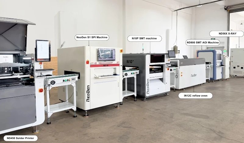
Solder Paste Printer -----> SPI Inspection Equipment -----> Pick-and-Place Machine -----> Reflow Oven -----> AOI Inspection

How Does SMT SPI Work?
The inspection workflow for a standard 3D SPI system typically consists of four steps:
Track Conve ───► Mark Camera Alignment ───► 3D Raster Scan ───► Pass/Fail & Report
1. PCB Entry into the SPI Equipment
The PCB enters the SPI machine via an automated track, where a clamping and positioning mechanism secures it to the optical inspection platform.
- Selection Guide: The NeoDen S1 supports PCB sizes ranging from a minimum of 50 × 50 mm to a maximum of 500 × 460 mm, with board thicknesses from 0.6 to 6 mm, covering the vast majority of industrial control, automotive electronics, and consumer electronics boards.
2. Mark Alignment and PCB Identification
An industrial camera locates and aligns with preset mark points on the PCB, correcting minor positional deviations and deformations that occur during conveyance. The NeoDen S1 supports the definition of multiple commonly used mark points (e.g., Mark 0, Mark 1), allowing for quick optical alignment calibration directly within the software interface.
3. 3D Vision-Based Solder Paste Data Acquisition
The system uses a 3D optical camera (such as a 3D raster camera with raster projection) to project a raster pattern onto the scanned area. By utilizing the principles of optical phase shift and triangulation, it captures three-dimensional topographic information of the solder paste surface. The NeoDen S1 simultaneously provides real-time display of both 2D and 3D true-color images, enabling intuitive visualization of measurement data.
4. Output of Inspection Results and SPC Data
SPI equipment not only outputs real-time OK/NG results for individual pads but also aggregates full-board data for Statistical Process Control (SPC). The NeoDen S1 offers powerful Offline SPC and SPC Report functions, supporting the export of comprehensive inspection data-including volume, area, height, and offset-to formats such as Excel, JPG, and BMP, facilitating quality traceability and process improvement.
What is the difference between 2D SPI and 3D SPI?
1. When selecting solder paste inspection equipment, many engineers often ask: What exactly is the difference between 2D SPI and 3D SPI?
| Comparison Dimensions | 2D SPI Equipment | 3D SPI Equipment |
| Vision Technology | Single/multi-angle planar camera image capture | 3D Raster/Structured Light |
| Inspection Dimensions | Planar Information (X/Y axes) | 3D Spatial Information (X/Y/Z axes) |
| Core Measurement Parameters | Coverage area, shape, planar position offset | Height, Volume, Area, Offset, 3D Topography |
| Height Measurement Capability | None (cannot accurately determine solder paste thickness) | Extremely high (accuracy up to 1 μm) |
| Defect Detection Rate | Prone to missing thickness-related defects such as collapse, peak formation, and thin spots | Comprehensive detection; accurately identifies soldering defects caused by excessive or insufficient volume |
2. Why is 3D solder paste inspection gaining increasing attention in SMT production?
In traditional enlarged pad processes, 2D measurement may meet basic requirements. However, when dealing with ultra-miniature components (such as 01005) or fine-pitch assemblies, minute variations in solder paste height and volume are often the primary causes of soldering defects. Thickness data cannot be obtained from two-dimensional images alone. Therefore, 3D SPI equipment equipped with a 3D raster camera has become the industry standard for modern, high-quality SMT production lines.
What is the difference between SPI and AOI?
This is one of the most common points of confusion in SMT procurement and process planning. Although both are automated visual inspection systems, they play distinctly different roles on the production line:
| Comparison | SPI (Solder Paste Inspection) | AOI (Automated Optical Inspection) |
| Primary Inspection Targets | Solder paste after printing | Surface-mounted components and solder joints after placement |
| Primary Inspection Stage | After the solder paste printer, before the placement machine | After component placement (pre-reflow AOI) or after reflow soldering (post-reflow AOI) |
| Typical Inspection Criteria | Volume, Area, Height, Offset | Visual defects such as missing components, incorrect components, reversed polarity, tombstoning, cold solder joints, and short circuits |
| Primary Functional Roles | Upstream Prevention: Intercept printing issues before component placement to reduce rework costs | Downstream Quality Control: Inspect the quality of the final assembly and soldered products |
Conclusion: SPI and AOI are not mutually exclusive; rather, they form a complementary "dual quality defense line."
How to Select SMT SPI Equipment?
When evaluating and procuring SPI equipment, it is recommended that process engineers and procurement teams focus on the following aspects:
1. Inspection Method: 2D or 3D?
If the factory handles PCBs containing fine-pitch BGAs, QFNs, or micro-components smaller than 0201, priority should be given to 3D SPI solutions capable of measuring three-dimensional topography, volume, and height.
2. Inspection Accuracy and Speed
Pay attention to the equipment's field of view (FOV), height measurement accuracy, repeatability, and processing speed.
3. PCB Size and Thickness Compatibility
Verify that the equipment's conveyor track range covers the factory's current and future PCB specifications. The NeoDen S1 supports PCB sizes up to 500 × 460 mm and board thicknesses ranging from 0.6 to 6 mm, offering broad workpiece adaptability.
4. Software, Programming, and Data Management Capabilities
Efficient software can significantly shorten new product introduction (NPI) time. Consider whether the equipment supports:
- Quick import of Gerber/CAD data
- Offline programming and manual programming
- SPC data analysis and multi-format report export (Excel/JPG/BMP)
Core Advantages of the NeoDen S1 SMT SPI System
As a 3D SPI solution specifically designed for high-efficiency SMT production lines, the NeoDen S1 integrates numerous outstanding features at both the hardware and software levels:
| NeoDen S1 Core Advantages | |
| 3D Raster Scan Visual Technology | High precision: 1 μm; supports 2D/3D true color |
| Full-Dimensional Geometric Parameter Measurement | Volume / Area / Height / Offset |
| Flexible and Fast Programming Logic | Gerber/CAD Import, Offline/Manual Programming |
| In-depth SPC data management | Export to Excel/JPG/BMP for full traceability |
1. 3D Raster Camera Visual Inspection System: Utilizes a high-precision 3D raster camera combined with 2D/3D true-color image display to clearly and intuitively reproduce the actual three-dimensional morphology of the solder paste.
2. Precise Detection of Volume, Area, Height, and Offset: A high-sensitivity optical measurement engine with a repeatability accuracy of less than 1 μm effectively detects even the rarest microscopic printing defects.
3. Gerber, CAD, and Offline Programming Support: Supports automatic parsing of Gerber and CAD files. Combined with the offline programming feature, programming preparations can be completed without tying up production line equipment, maximizing production line utilization.
4. SPC Data Analysis and Multi-Format Reporting: The system features built-in Offline SPC functionality, allowing engineers to access "Anytime Reports" at any time and export reports to Excel, JPG, or BMP formats with a single click, meeting the quality traceability requirements of high-end client factories.
5. User-Friendly Operation Workflow and Customizable Settings: As outlined in the operating manual, the NeoDen S1 provides a clear step-by-step guide:
Define Mark Points ---> Load Inspection Path ---> Set Stencil/Pad Thresholds ---> Select Detection Type ---> Start Automatic Inspection
Which SMT production scenarios are suitable for SPI?
1. Mass-Production PCB Automation
As production volumes increase and product models change frequently, relying on manual visual inspection of solder paste is not only inefficient but also prone to fatigue-induced missed defects. Introducing 3D SPI enables 100% fully automated and rapid inspection.
2. Fine-Pitch and High-Density PCB Assembly
For complex boards containing fine-pitch components such as 01005 SMDs, BGAs, CSPs, and QFNs, the consistency of solder paste printing directly determines soldering yield. 3D SPI is essential equipment for ensuring the success of such precision processes.
3. Modern Factories Aiming for Zero Defects and Data Traceability
In the manufacturing of automotive electronics, medical devices, industrial control systems, and communications equipment, customers often require complete SPC process data traceability. The quality data exported by SPI systems is a key factor in factory ratings and customer audits.
SMT SPI Equipment Frequently Asked Questions (FAQ)
Q1: What does SPI stand for?
A: SPI stands for Solder Paste Inspection, which refers to equipment specifically designed to inspect the quality of solder paste after the SMT printing process.
Q2: What does SPI equipment primarily inspect?
A: It primarily inspects three-dimensional geometric parameters such as the volume, area, height, and planar position offset of the solder paste after PCB printing.
Q3: Is 3D inspection mandatory for SPI?
A: Not necessarily, but 3D is the trend. 2D SPI can only inspect planar area and position; it cannot capture critical height and volume data.
For SMT production lines handling high-density, micro-components, the use of 3D SPI is strongly recommended.
Q4: Can SPI and AOI be used interchangeably?
A: No. SPI inspects solder paste after printing and serves as a pre-process preventive measure; AOI inspects components and solder joints after placement or soldering and acts as a post-process quality control measure. The two work in tandem within the SMT quality system.
Q5: Where should SPI be positioned on the SMT production line?
A: It must be placed after the solder paste printer and before the placement machine.
Q6: What key parameters should be considered when selecting SPI equipment?
A: We recommend focusing on: inspection technology (2D/3D), field of view (FOV), height measurement accuracy, repeatability, processing speed, PCB size and thickness compatibility, programming methods (Gerber/CAD/offline), and the ability to generate SPC data reports.

Conclusion
The core value of SPI is by no means limited to simply "identifying defective boards"; more importantly, it enables process engineers to obtain precise, quantifiable 3D printing data prior to placement. By using SPC traceability feedback to guide parameter optimization of the printer, potential quality issues can be eliminated before they arise.
Explore NeoDen's Smart SMT Solutions
Click to view detailed specifications for the NeoDen S1 3D SPI solder paste inspection system.